I’ve been having problems with layout. I will detail them at the bottom. For now, I’ll show the results of what works first and describe the problems.
Transistor Level Design & Simulation

These are the ELDO results for a NOR2 gate constructed using the DK transistors via schematic capture. So, we can construct our own custom gates and simulate them. However, I was unable to get SDL working for this design. Note: It took a while to get this working as ICNET was not getting the W/L information from the INSTPAR property. We need to specify a W and L property for each transistor to get the simulation models to work. We can use the default MN and MP symbols from Mentor as long as we set the appropriate ASIM_MODEL, W and L properties.
The DK provides TYP, SLOW, FAST transistor models. These files (in $MTC_CMOS05/analog/) need to be included in the final SPICE netlist. This can be specified from the simulation menus. The models used here are the EN and EP models. There is also a ENMM9 and EPMM9 model (Philips MM9) in the library that we can use. The SGS-Thompson models in the library cannot be used as we do not have the license for it.
Analogue Design & Simulation

As you can see, ELDO simulation of a NOR2_RING works. The design is made up of instances of the NOR2 above, laid out in a RING via schematic capture. So, it is possible to capture a hierarchical design in a schematic, and simulate it. This is only useful for designs constructed from scratch. The DK does not provide schematic level simulation data for the standard cells. It only provides compiled digital models. So, it is only possible to do complex gate-level simulation digitally. This should be okay as long as we limit the analogue simulation to our custom NOR2 gate.
Digital Design & Simulation
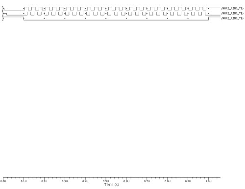
As you can see, the digital simulation works as well. This is a MODELSIM simulation of the RING oscillator that was designed via schematic capture. However, instead of simulating the transistor models, the NOR2 gate above is described using a VHDL model. It was important to test this as there are VHDL simulation models for all the DK standard cells. Even if we do not get Leonardo working, it would still be possible to construct a design using the standard cells by performing synthesis by hand of simple designs.
It should be possible to enter the design as a schematic (as is done in the present VLSI project) and construct basic building blocks (counters, shift registers and other blocks). Then, it should hopefully be possible to instantiate the DK simulation models. I have tried simulating the DK models and they work. However, I have yet to try instantiating the DK models from within a schematic capture for digital simulation.
I have also yet to try building a design and simulating it from a purely VHDL netlist. This should work as we are allowed to IMPORT a VHDL netlist from within ICSTUDIO. I will need to try this next.
What DOES NOT Work
At the moment, the biggest head-ache is layout. It is possible to directly run SDL for the standard cells by modifying the existing DK. I am still unable to get the internal device generator to work, in order to layout transistors directly. This may have something to do with another missing property for the transistors, or it may be something else. I’ll try to get this to work. If this can work, we can at least bring the design of a single NOR2 gate from start to finish.
Although I am able to run SDL for the standard cells, I am unable to get FLOORPLANNING nor AUTOCELLS to work. So, the standard cells are laid out according to their positions in the schematic. This means that there will be a lot of manual cajoling required. I do not know why these things do not work. Hopefully, I’ll figure it out soon.
What We CAN do
- Design the whole design using standard cells in a schematic or possibly, a low-level VHDL netlist. We can simulate it at the gate-level with digital simulation and layout the design using the standard cells via SDL.
- Design a custom NOR2 using standard transistors. This will fall short of the full design flow as we cannot yet do the transistor level SDL layout.
What is UNKNOWN
For some reason, Calibre has popped up in the menus. As I am yet unable to do a transistor level layout, I have yet to test the DRC, XRC processes. I have also not been able to test BACK-ANNOTATION nor digital simulation with SDL (delay) data. I will try to get layout working and ascertain if Calibre works.

Some very interesting developments. I would have laid a short bet SDL would work with cells but not with transistors. I am not surpised though that the DK needs adaptation. Full S-D-layout tr-level seems v slow in actually coming properly even though i first saw it abt 20 yrs ago
What do you think is the probability of having a project that could be used on the ugrads in may 08? Hugh Shercliff is keen to report to the Teaching committee on Monday.